 | –≠–ª–µ–∫—Ç—Ä–æ–Ω–Ω—ã–π –∫–æ–º–ø–æ–Ω–µ–Ω—Ç: LTC3406 | –°–∫–∞—á–∞—Ç—å:  PDF PDF  ZIP ZIP |
LTC3548
1
3548f
, LTC and LT are registered trademarks of Linear Technology Corporation. All other
trademarks are the property of their respective owners. Burst Mode is a registered
trademark of Linear Technology Corporation. Protected by U.S. Patents including 5481178,
6580258, 6304066, 6127815, 6498466, 6611131.
APPLICATIO S
U
FEATURES
TYPICAL APPLICATIO
U
DESCRIPTIO
U
PDAs/Palmtop PCs
Digital Cameras
Cellular Phones
Portable Media Players
PC Cards
Wireless and DSL Modems
High Efficiency: Up to 95%
Very Low Quiescent Current: Only 40µA
2.25MHz Constant Frequency Operation
High Switch Current: 0.7A and 1.2A
No Schottky Diodes Required
Low R
DS(ON)
Internal Switches: 0.35
Current Mode Operation for Excellent Line
and Load Transient Response
Short-Circuit Protected
Low Dropout Operation: 100% Duty Cycle
Ultralow Shutdown Current: I
Q
< 1µA
Output Voltages from 5V down to 0.6V
Power-On Reset Output
Externally Synchronizable Oscillator
Small Thermally Enhanced MSOP and 3mm ◊ 3mm
DFN Packages
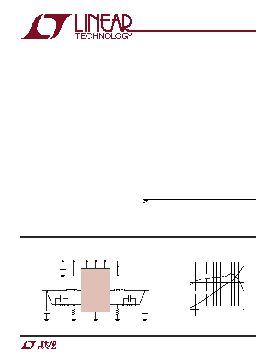
Dual Synchronous,
400mA/800mA, 2.25MHz
Step-Down DC/DC Regulator
The LTC
Æ
3548 is a dual, constant frequency, synchronous
step down DC/DC converter. Intended for low power
applications, it operates from 2.5V to 5.5V input voltage
range and has a constant 2.25MHz switching frequency,
allowing the use of tiny, low cost capacitors and inductors
with a profile 1.2mm. Each output voltage is adjustable
from 0.6V to 5V. Internal synchronous 0.35, 0.7A/1.2A
power switches provide high efficiency without the need
for external Schottky diodes.
A user selectable mode input is provided to allow the user
to trade-off noise ripple for low power efficiency. Burst
Mode
Æ
operation provides high efficiency at light loads,
while Pulse Skip Mode provides low noise ripple at light
loads.
To further maximize battery runtime, the P-channel
MOSFETs are turned on continuously in dropout (100%
duty cycle), and both channels draw a total quiescent
current of only 40µA. In shutdown, the device draws <1µA.
LTC3548 Efficiency Curve
Figure 1. 2.5V/1.8V at 400mA/800mA Step-Down Regulators
RUN2
V
IN
V
IN
= 2.8V
TO 5.5V
V
OUT2
= 2.5V
AT 400mA
V
OUT1
= 1.8V
AT 800mA
RUN1
POR
SW1
V
FB1
GND
V
FB2
SW2
MODE/SYNC
LTC3548
10µF
100k
RESET
33pF
68pF
2.2µH
4.7µH
887k
604k
301k
280k
4.7µF
10µF
3548 TA01
LOAD CURRENT (mA)
1
EFFICIENCY (%)
100
95
90
85
80
75
70
65
60
POWER LOSS (mW)
1000
100
10
1
0.1
10
100
1000
3548 TA02
V
IN
= 3.3V, V
OUT
= 1.8V
Burst Mode OPERATION
CHANNEL 1, NO LOAD ON CHANNEL 2
POWER LOSS
EFFICIENCY
LTC3548
2
3548f
TOP VIEW
DD PACKAGE
10-LEAD (3mm ◊ 3mm) PLASTIC DFN
DD PIN 11, EXPOSED PAD: PGND
MUST BE CONNECTED TO GND
10
11
9
6
7
8
4
5
3
2
1
V
FB2
RUN2
POR
SW2
MODE/
SYNC
V
FB1
RUN1
V
IN
SW1
GND
V
IN
Voltages .................................................≠ 0.3V to 6V
V
FB1
, V
FB2
, RUN1, RUN2
Voltages ..................................... ≠ 0.3V to V
IN
+ 0.3V
MODE/SYNC Voltage ...................... ≠ 0.3V to V
IN
+ 0.3V
SW1, SW2 Voltage ......................... ≠ 0.3V to V
IN
+ 0.3V
POR Voltage ................................................≠ 0.3V to 6V
ABSOLUTE AXI U
RATI GS
W
W
W
U
(Note 1)
ELECTRICAL CHARACTERISTICS
The
denotes the specifications which apply over the full operating
temperature range, otherwise specifications are at T
A
= 25∞C. V
IN
= 3.6V, unless otherwise specified. (Note 2)
SYMBOL
PARAMETER
CONDITIONS
MIN
TYP
MAX
UNITS
V
IN
Operating Voltage Range
2.5
5.5
V
I
FB
Feedback Pin Input Current
30
nA
V
FB
Feedback Voltage (Note 3)
0∞C T
A
85∞C
0.588
0.6
0.612
V
≠40∞C T
A
85∞C
0.585
0.6
0.612
V
V
LINE REG
Reference Voltage Line Regulation
V
IN
= 2.5V to 5.5V (Note 3)
0.3
0.5
%/V
V
LOAD REG
Output Voltage Load Regulation
(Note 3)
0.5
%
I
S
Input DC Supply Current
Active Mode
V
FB1
= V
FB2
= 0.5V
700
950
µA
Sleep Mode
V
FB1
= V
FB2
= 0.63V, MODE/SYNC = 3.6V
40
60
µA
Shutdown
RUN = 0V, V
IN
= 5.5V, MODE/SYNC = 0V
0.1
1
µA
f
OSC
Oscillator Frequency
V
FB
= 0.6V
1.8
2.25
2.7
MHz
f
SYNC
Synchronization Frequency
2.25
MHz
I
LIM
Peak Switch Current Limit Channel 1
V
IN
= 3V, V
FB
= 0.5V, Duty Cycle <35%
0.95
1.2
1.6
A
Peak Switch Current Limit Channel 2
V
IN
= 3V, V
FB
= 0.5V, Duty Cycle <35%
0.6
0.7
0.9
A
R
DS(ON)
Top Switch On-Resistance
(Note 6)
0.35
0.45
Bottom Switch On-Resistance
(Note 6)
0.30
0.45
I
SW(LKG)
Switch Leakage Current
V
IN
= 5V, V
RUN
= 0V, V
FB
= 0V
0.01
1
µA
Ambient Operating Temperature
Range (Note 2) ................................... ≠ 40∞C to 85∞C
Junction Temperature (Note 5) ............................. 125∞C
Storage Temperature Range ................. ≠ 65∞C to 125∞C
Lead Temperature (Soldering, 10 sec)
LTC3548EMSE only .......................................... 300∞C
ORDER PART
NUMBER
DD PART MARKING
T
JMAX
= 125∞C,
JA
= 45∞C/W,
JC
= 3∞C/W
(Soldered to a 4-layer board)
LBNJ
LTC3548EDD
PACKAGE/ORDER I FOR ATIO
U
U
W
Consult LTC Marketing for parts specified with wider operating temperature ranges.
ORDER PART
NUMBER
MSE PART MARKING
T
JMAX
= 125∞C,
JA
= 45∞C/W,
JC
= 10∞C/W
(Soldered to a 4-layer board)
LTBNH
LTC3548EMSE
TOP VIEW
1
2
3
4
5
V
FB1
RUN1
V
IN
SW1
GND
10
9
8
7
6
V
FB2
RUN2
POR
SW2
MODE/
SYNC
11
MSE PACKAGE
10-LEAD PLASTIC MSOP
MSE PIN 11, EXPOSED PAD: PGND
MUST BE CONNECTED TO GND
LTC3548
3
3548f
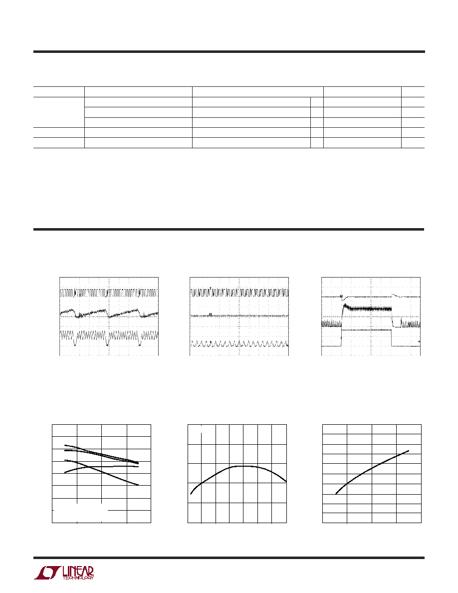
2.5
2.4
2.3
2.2
2.1
2.0
FREQUENCY (MHz)
10
8
6
4
2
0
≠ 2
≠ 4
≠ 6
≠ 8
≠10
FREQUENCY DEVIATION (%)
SUPPLY VOLTAGE (V)
2
3548 G06
3
4
5
6
INPUT VOLTAGE (V)
2
3548 G04
3548 G01
3548 G02
3548 G03
3
4
5
6
TEMPERATURE (∞C)
≠50
25
75
3548 G05
≠25
0
50
100
125
100
95
90
85
80
75
70
65
60
EFFICIENCY (%)
V
IN
= 3.6V
V
OUT
= 1.8V
I
LOAD
= 180mA
CHANNEL 1; CIRCUIT OF FIGURE 3
V
IN
= 3.6V
V
OUT
= 1.8V
I
LOAD
= 30mA
CHANNEL 1; CIRCUIT OF FIGURE 3
V
IN
= 3.6V
V
OUT
= 1.8V
I
LOAD
= 80mA TO 800mA
CHANNEL 1; CIRCUIT OF FIGURE 3
V
OUT
= 1.8V, CHANNEL 1
Burst Mode OPERATION
CIRCUIT OF FIGURE 3
800mA
10mA
100mA
1mA
SW
5V/DIV
V
OUT
20mV/DIV
I
L
200mA/DIV
SW
5V/DIV
V
OUT
10mV/DIV
I
L
200mA/DIV
V
OUT
200mV/DIV
I
L
500mA/DIV
I
LOAD
500mA/DIV
2µs/DIV
1µs/DIV
20µs/DIV
V
IN
= 3.6V
TYPICAL PERFOR A CE CHARACTERISTICS
U
W
Load Step
Burst Mode Operation
Pulse Skipping Mode
Efficiency vs Input Voltage
Oscillator Frequency vs Supply
Voltage
Oscillator Frequency vs
Temperature
Note 1: Absolute Maximum Ratings are those values beyond which the life
of a device may be impaired. No pin shall exceed 6V.
Note 2: The LTC3548 is guaranteed to meet specified performance from
0∞C to 70∞C. Specifications over the ≠ 40∞C and 85∞C operating
temperature range are assured by design, characterization and correlation
with statistical process controls.
Note 3: The LTC3548 is tested in a proprietary test mode that connects
V
FB
to the output of the error amplifier.
Note 4: Dynamic supply current is higher due to the internal gate charge
being delivered at the switching frequency.
Note 5: T
J
is calculated from the ambient T
A
and power dissipation P
D
according to the following formula: T
J
= T
A
+ (P
D
∑
JA
).
Note 6: The DFN switch on-resistance is guaranteed by correlation to
wafer level measurements.
ELECTRICAL CHARACTERISTICS
The
denotes the specifications which apply over the full operating
temperature range, otherwise specifications are at T
A
= 25∞C. V
IN
= 3.6V, unless otherwise specified. (Note 2)
SYMBOL
PARAMETER
CONDITIONS
MIN
TYP
MAX
UNITS
POR
Power-On Reset Threshold
V
FB
Ramping Down, MODE/SYNC = 0V
≠8.5
%
Power-On Reset On-Resistance
100
200
Power-On Reset Delay
262,144
Cycles
V
RUN
RUN Threshold
0.3
1
1.5
V
I
RUN
RUN Leakage Current
0.01
1
µA
T
A
= 25∞C unless otherwise specified.
LTC3548
4
3548f
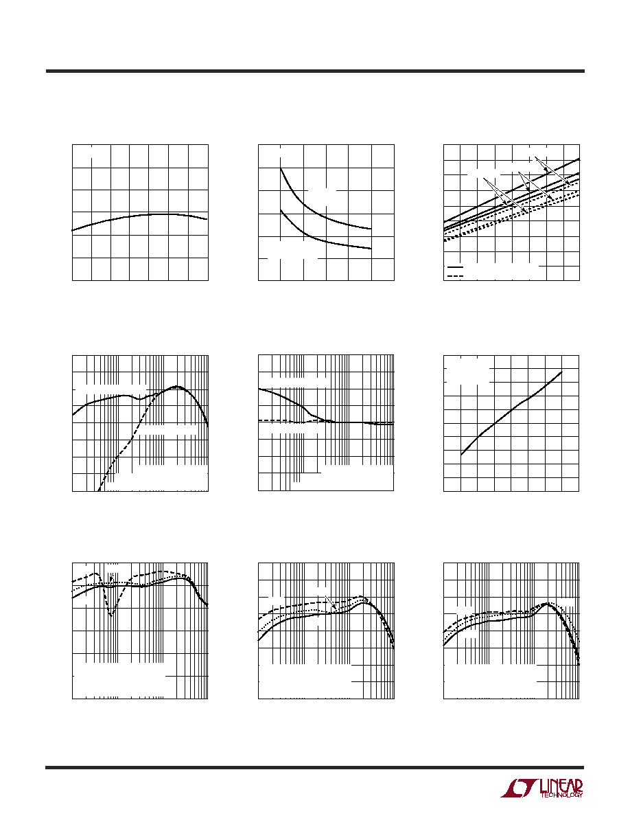
V
IN
(V)
2
V
OUT
ERROR (%)
0.5
0.4
0.3
0.2
0.1
0
≠0.1
≠0.2
≠0.3
≠0.4
≠0.5
4
6
3548 G15
3
5
V
OUT
= 1.8V
I
OUT
= 200mA
T
A
= 25∞C
V
IN
(V)
1
500
450
400
350
300
250
200
4
6
3548 G08
2
3
5
7
R
DS(ON)
(m
)
MAIN
SWITCH
SYNCHRONOUS
SWITCH
0.615
0.610
0.605
0.600
0.595
0.590
0.585
REFERENCE VOLTAGE (V)
JUNCTION TEMPERATURE (∞C)
≠50
550
500
450
400
350
300
250
200
150
100
25
75
3548 G09
≠25
0
50
100
150
125
TEMPERATURE (∞C)
≠50
25
75
3548 G07
≠25
0
50
100
125
R
DS(ON)
(m
)
MAIN SWITCH
SYNCHRONOUS SWITCH
V
IN
= 3.6V
V
IN
= 3.6V
V
IN
= 4.2V
V
IN
= 2.7V
T
A
= 25∞C
LOAD CURRENT (mA)
1
EFFICIENCY (%)
100
90
80
70
60
50
40
10
100
1000
3548 G10
3.6V
2.7V
4.2V
V
OUT
= 2.5V, CHANNEL 1
Burst Mode OPERATION
NO LOAD ON OTHER CHANNEL
CIRCUIT OF FIGURE 3
LOAD CURRENT (mA)
1
EFFICIENCY (%)
100
95
90
85
80
75
70
65
60
10
100
1000
3548 G13
2.7V
4.2V
V
OUT
= 1.2V, CHANNEL 1
Burst Mode OPERATION
NO LOAD ON OTHER CHANNEL
CIRCUIT OF FIGURE 3
LOAD CURRENT (mA)
1
EFFICIENCY (%)
100
95
90
85
80
75
70
65
60
10
100
1000
3548 G14
2.7V
4.2V
LOAD CURRENT (mA)
1
EFFICIENCY (%)
100
95
90
85
80
75
70
65
60
10
100
1000
3548 G11
V
IN
= 3.6V, V
OUT
= 1.8V
NO LOAD ON OTHER CHANNEL
CHANNEL 1; CIRCUIT OF FIGURE 3
LOAD CURRENT (mA)
1
V
OUT
ERROR (%)
2.0
1.5
1.0
0.5
0
≠0.5
≠1.0
≠1.5
≠2.0
10
100
1000
3548 G12
Burst Mode OPERATION
Burst Mode OPERATION
PULSE SKIP MODE
PULSE SKIP MODE
V
OUT
= 1.5V, CHANNEL 1
Burst Mode OPERATION
NO LOAD ON OTHER CHANNEL
CIRCUIT OF FIGURE 3
3.6V
3.6V
V
IN
= 3.6V, V
OUT
= 1.8V
NO LOAD ON OTHER CHANNEL
CHANNEL 1; CIRCUIT OF FIGURE 3
Efficiency vs Load Current
Load Regulation
Line Regulation
Efficiency vs Load Current
Efficiency vs Load Current
Efficiency vs Load Current
TYPICAL PERFOR A CE CHARACTERISTICS
U
W
Reference Voltage vs
Temperature
R
DS(ON)
vs Input Voltage
R
DS(ON)
vs Junction Temperature

LTC3548
5
3548f
V
FB1
(Pin 1): Output Feedback. Receives the feedback
voltage from the external resistive divider across the
output. Nominal voltage for this pin is 0.6V.
RUN1 (Pin 2): Regulator 1 Enable. Forcing this pin to V
IN
enables regulator 1, while forcing it to GND causes regu-
lator 1 to shut down. This pin must be driven; do not float.
V
IN
(Pin 3): Main Power Supply. Must be closely decoupled
to GND.
SW1 (Pin 4): Regulator 1 Switch Node Connection to the
Inductor. This pin swings from V
IN
to GND.
GND (Pin 5): Main Ground. Connect to the (≠) terminal of
C
OUT
, and (≠) terminal of C
IN
.
MODE/SYNC (Pin 6): Combination Mode Selection and
Oscillator Synchronization. This pin controls the operation
of the device. When tied to V
IN
or GND, Burst Mode
operation or pulse skipping mode is selected, respec-
tively. Do not float this pin. The oscillation frequency can
U
U
U
PI FU CTIO S
be synchronized to an external oscillator applied to this pin
and pulse skipping mode is automatically selected.
SW2 (Pin 7): Regulator 2 Switch Node Connection to the
Inductor. This pin swings from V
IN
to GND.
POR (Pin 8): Power-On Reset . This common-drain logic
output is pulled to GND when the output voltage falls
below ≠8.5% of regulation and goes high after 117ms
when both channels are within regulation.
RUN2 (Pin 9): Regulator 2 Enable. Forcing this pin to V
IN
enables regulator 2, while forcing it to GND causes regu-
lator 2 to shut down. This pin must be driven; do not float.
V
FB2
(Pin 10): Output Feedback. Receives the feedback
voltage from the external resistive divider across the
output. Nominal voltage for this pin is 0.6V.
Exposed Pad (GND) (Pin 11): Power Ground. Connect to
the (≠) terminal of C
OUT
, and (≠) terminal of C
IN
. Must be
connected to electrical ground on PCB.